| |
Manufacture capacity |
|
| engineering technology category |
engineering capacity |
tolerance range (standard) |
| board |
FR-4&RCC |
NA |
| wire etching capacity |
Width:3mil; Space:3mil |
>=10mil,+/-2mil,<10mil,+/-20% |
| machinery aperture processing capacity |
PTH |
φ0.20mm |
+/-0.075mm |
| N-PTH |
φ0.20mm |
+/-0.075mm |
| Laset |
φ0.10mm |
+/-0.075mm |
| layer number of multilayer board |
board of 2-20 layers |
NA |
| the thickness of anti-flux |
>=0.4mil |
NA |
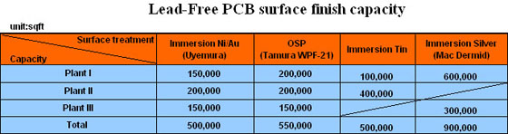
| surface treatment |
chemical electroless gold |
NA |
| spray tin |
| chemical electroless silver |
| chemical electroless tin |
| gold plating |
| impedance request |
controllable |
NA |
| molding processing |
nc ROUTING |
+/-4mil(+/-0.1mm) |